
MEMS platform based on wafer bonding
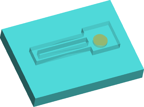
Some MEMS devices have to be built of more than 1 substrates. The different substrates are integrated either at the final phase by assembly process or at the initial phase by wafer-level bonding process. Assembly process is relatively easier to achieve, however, it is a labour hungry technique. The latter process gives a significant advantage in term of batch fabrication, and thus, reducing overall device fabrication cost. We are developing MEMS process platforms utilizing the wafer bonding process to enable batch fabrication of the devices.
単独の基板から作成されるデバイスも有りながら、複数の基板から作成されるデバイスも存在する。複数の基板から作成された場合、いずれかの最後に組み立てられるか、あるいは最初から接合される。組立プロセスと比べ、接合プロセスによって量産化ができるという利点があり、低コスト化もできる。我々は、ガラスとガラス及びシリコンとシリコンの基板を接合し、MEMSプロセスプラットフォームを開発した。特に、ガラスは低膨張率を持つため、MEMS共振子としての熱ロスを低下するためには望ましい材料。更に、ウェハ接合によって、基板間のギャップの制御もできた。開発したプロセスプラットフォームを用いてジャイロセンサー用の円型共振子や面内外共振子を開発した。
Related publications:
- M. J. Khan, T. Tsukamoto, M. S. Al Farisi, S. Tanaka: “Fabrication Method of Micromachined Quartz Glass Resonator Using Sacrificial Supporting Structures,” Sens. Act. A Phys. 305, p. 111922 (2020).